Generating Analog Signals from Microcontrollers: A Practical Guide
In this post, we will discuss how to get an analog signal out of our microcontroller.
To produce a control voltage for our modular synth, we need a circuit that can convert a digital value—like an audio sample, MIDI CC, or mapped value—into an analog signal. This type of circuit is called a digital-to-analog converter, or DAC. There are many types of DACs, and choosing the right one can be a bit intimidating. Fortunately, many of these DAC circuits are available as integrated circuits (ICs) that share common communication protocols like I2C and SPI. If you’re interested in exploring the various types of DACs, check out the links in the resources section at the end of this post.
Some microcontrollers, like the Teensy and Daisyseed, come with integrated DAC outputs. Others, like the STM32 we’re using today, require an external component. For this post, we’ll be working with the MCP4822, a 12-bit DAC IC that I happen to have on hand.
Another way to generate an analog signal from a microcontroller is by using PWM through a low-pass filter. While this method has some drawbacks—such as lower resolution or potential audible artifacts—you can achieve higher resolution by combining two PWM output pins. With the right filter circuits, you can ensure an acceptably clean output signal too.
Since today’s topic explores control voltage, this is an excellent opportunity to also discuss how to generate such a signal with code. When generating an analog signal within the realm of computers and microcontrollers, our options boil down to this:
- Generate the signal in real-time by making use of algorithms to calculate the wave samples on every loop cycle.
- Render the audio using pre-calculated values stored in a value map.
Of course, the first method offers a much more accurate waveform generation, but with a catch: it has a much higher computational cost. Since we are dealing with microcontrollers, this is not trivial at all. The latter method, on the other hand, has a very low computational cost but requires data storage to hold the pre-calculated values, typically in the form of RAM. Also, depending on the number of pre-calculated values, we may sacrifice some fidelity. However, we can utilize a technique called interpolation to improve the fidelity of a generated signal by calculating in-between values, allowing us to use less RAM. But, the name of the game here is “finding the right balance.”
Today, we will use this latter method, and because we are good developers, we’ll encapsulate the functionality of both the DAC IC and PWM into a common interface, which allows us to easily swap between the two methods.
Let’s get started.
Part 1: On the MCP4822 DAC
The best way to get started is by visiting the IC’s datasheet! You’ll find all sorts of great information about your device. Take a look a these secions in particular as they hold information we need in order to ensure our circuit performs as expected.
Key Datasheet Sections
- Block Diagram: This provides a logical view into the inner workings of the IC. One particularly interesting feature is the internal output buffers. This mean we don’t need additional components to ensure our outputs have a dedicated current source. All we need is a 1K current-limiting resistor on the output—nice and simple!
- Power Requirements: Look for the “Absolute Maximum Ratings” to understand the power limits. The MCP4822 can handle up to 6.5V, but according to the electrical characteristics table, the safe VDD range is 2.7V to 5.5V. To get the maximum output voltage of 4.096V (rail-to-rail), power the IC with 5V. NOTE: To ensure compatibility with a standard Eurorack power bus, we’ll include a voltage regulator IC to convert the 12V rail to 5V, which will then power the MCP4822.
- Supply Considerations: This section provides guidelines on how to wire the IC to power, including the use of decoupling capacitors and their recommended values.
- Layout Considerations: Check the “Typical Connection Diagram” for a clear illustration of how to wire up the IC.
- Serial Interface: This section explains how to write data to the DAC. To use the DAC, first, select the desired DAC by pulling the CS pin low, then send the 16-bit data word, and finally pull the CS pin high to complete the write operation and update the DAC output. The the video link the references section for a detailed explanation of the SPI interface.
Wiring the MCP4822
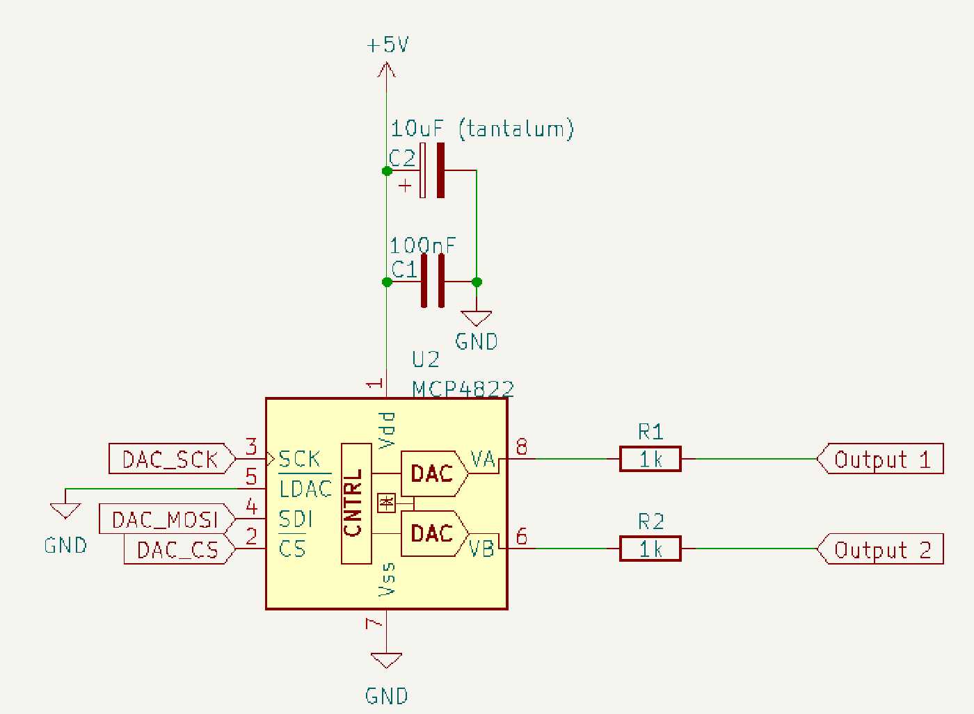
- Connect pin 7 (VSS) to Ground.
- Connect pin 1 (VDD) to a 5V source.
- Add bypass capacitors as close to pin 1 as possible:
- A 0.1uF ceramic capacitor.
- A 10uF tantalum capacitor (be careful with polarity; connect the negative lug to GND).
- Connect pin 2 to the microcontroller’s CS pin.
- Connect pin 3 to the microcontroller’s SCK pin.
- Connect pin 4 to the microcontroller’s MOSI pin.
- Connect the outputs to jacks through a 1K current-limiting resistor.
- Connect pin 5 to GND.
Example Code using the Arduino Framework
This example will generate a simple ramp waveform on one of the DAC channels.
#include <SPI.h>

const int CS_PIN = PB12;  // Chip Select pin connected to PB12 on the Blue Pill

void setup() {
  // Initialize SPI communication
  SPI.begin();

  // Set the CS pin as output
  pinMode(CS_PIN, OUTPUT);

  // Set CS pin high to deselect the DAC
  digitalWrite(CS_PIN, HIGH);
}

void loop() {
  for (uint16_t value = 0; value < 4096; value++) {
    writeDAC(value, 0); // Write to channel A with the ramp value
    delay(1);           // Small delay to slow down the ramp for visibility
  }
}

// Function to write to the MCP4822 DAC
void writeDAC(uint16_t value, int channel) {
  uint16_t command = 0x3000; // Default command bits (0b0011 0000 0000 0000)

  if (channel == 1) {
    command |= 0x8000; // Set bit 15 to select channel B
  }

  command |= (value & 0x0FFF); // Mask the value to 12 bits and combine with the command

  // Select the DAC by pulling CS low
  digitalWrite(CS_PIN, LOW);

  // Send the command via SPI
  SPI.transfer16(command);

  // Deselect the DAC by pulling CS high
  digitalWrite(CS_PIN, HIGH);
}
How It Works
- Setup:
- SPI.begin() initializes the SPI communication.
- The CS pin is set as an output and pulled high to ensure the DAC is deselected.
- Loop:
- The loop iterates over values from 0 to 4095, which corresponds to the 12-bit resolution of the MCP4822.
- writeDAC(value, 0) sends these values to channel A, generating a ramp waveform.
- writeDAC Function:
- This function constructs the 16-bit command word required by the MCP4822.
- It then sends this command via SPI while managing the CS pin to select and deselect the DAC.
Notes:
Channel Selection: The code can write values to either channel A (0) or channel B (1) of the MCP4822.
Resolution: The MCP4822 has a 12-bit resolution, so the value ranges from 0 to 4095.
SPI Settings: The SPI settings here are the default for Arduino. If needed, you can adjust the clock speed and data order using SPISettings.
Part 2: On the Hi-Fi PWM DAC
One of the simplest methods to achieve analog output from a microcontroller is by using a single PWM pin, configuring it as an output, and passing it through a low-pass filter. Afterward, you can buffer the output and add a current-limiting resistor before the output jack. However, while straightforward, this approach won’t give us the best results, as I mentioned earlier.
To improve the quality of our output, we’ll combine two PWM pins and set different cutoff points before summing the two outputs into one. This effectively turns one pin into a coarse converter while the other handles the finer values. This technique, known as Hi-Fi mode, is well-documented in the Mozzi website. However, instead of directly using Mozzi’s implementation, we’ll borrow some relevant bits from Matias-Levi’s PWM version of Peaks. The circuit remains the same for the most part, but we’ll adapt the code to work with the Arduino Framework instead of STM32Cube.
Example Circuit and Special Considerations
Each analog output requires two PWM pins, and to ensure synchronization, these pins must use the same timer. For instance, when using the STM32 BluePill, you can use pins PB6, PB7, PB8, and PB9, all tied to Timer 4. In this configuration, for example:
- PB6 serves as PWM1 on Channel 1 (DAC A).
- PB7 serves as PWM2 on Channel 1 (DAC A).
- PB8 and PB9 will be used similarly for DAC B on Channel 2.
To find which timer and pins you should be using refer to the microcontroller’s datasheet as the pin layouts will be different depending on the device you are using.
Wiring diagram
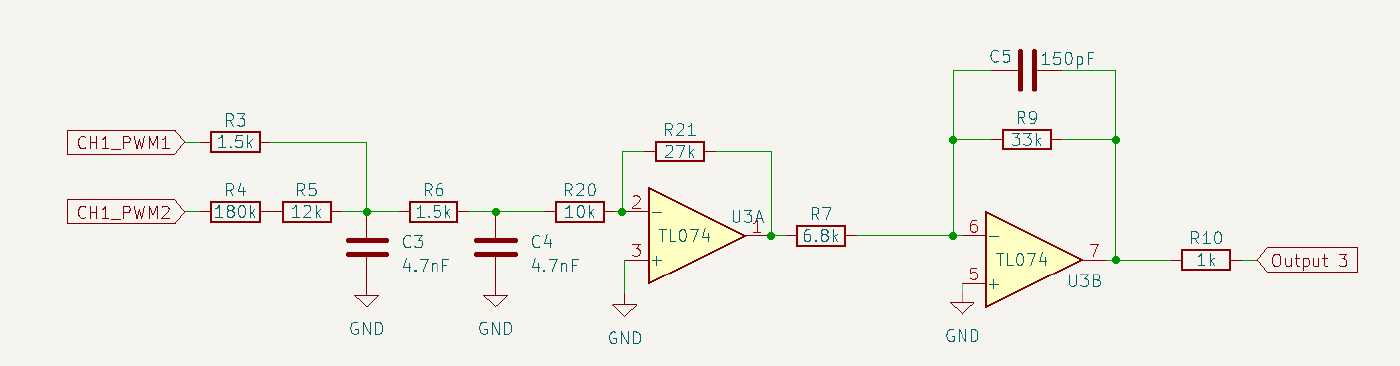
- Connect PB6 to a 1.5K resistor (R3).
- Connect PB7 to a 192K resistor (or a 180K and 12K resistor in series, as shown above; R4 and R5).
- Connect the other sides of R3 and R5 to a common node, and at this node, connect a 4.7nF capacitor to GND. This forms the first filter stage and effectively sums the two outputs into one.
- This combined output is then connected to a second low-pass filter stage using a 1.5K resistor and a 4.7nF capacitor to GND. The output of this stage is buffered with a general-purpose op-amp; a TL07X will work here. I’m using an inverting apmlifier to buffer and also invert and scale the signal.
- The buffered output is then pass through an active low pass filter which further helps ensure no high frequency noise makes it to the signal path.
- Note that after the first opamp the signal will be negative. This is also where you can introduce a positive voltage at half the amplitude of the signal so it can be centered on the 0v line if needed.
- The output of the op-amp is fed back to the inverting input through an RC network (33K resistor R9 and 150pF capacitor C5) This is the active low-pass filter.
- Warning: chaning the value of R7, R9 or C5 will change the filter’s cutoff. If you need to scale your signal do it at the first opamp stage by adjusting R21 instead.
- Finally, the output is connected to a jack through a 1K current-limiting resistor.
Example Code
Header file:
#ifndef PWM_DAC_H_
#define PWM_DAC_H_

#include <Arduino.h>
#include "stm32f1xx_hal.h"

// Use a PWM frequency of 125kHz instead of the default.
const uint32_t kPwmFrequency = 125000;
const uint16_t kPwmResolution = 7;

class PWMDac {
 public:
  PWMDac(TIM_TypeDef* timer, uint8_t pin1, uint8_t pin2, uint8_t pin3, uint8_t pin4);
  ~PWMDac();

  void Init();
  void Write(int index, uint16_t value);

 private:
  HardwareTimer* timer_;
  TIM_TypeDef* timerInstance_;
  uint8_t pin1_, pin2_, pin3_, pin4_;
  uint16_t data_[2];
};

#endif  // PWM_DAC_H_
Implementation file:
#include "PWMDac.h"

PWMDac::PWMDac(HardwareTimer& timer, uint8_t pin1, uint8_t pin2, uint8_t pin3, uint8_t pin4)
  : timer_(timer), pin1_(pin1), pin2_(pin2), pin3_(pin3), pin4_(pin4) { }

PWMDac::~PWMDac() { }

void PWMDac::Init() {
  // Initialize pins.
  pinMode(pin1_, OUTPUT);
  pinMode(pin2_, OUTPUT);
  pinMode(pin3_, OUTPUT);
  pinMode(pin4_, OUTPUT);

  // Set the PWM frequency for the pins.
  timer_.setPrescaleFactor(1);
  timer_.setOverflow(kPwmFrequency, HERTZ_FORMAT);
  timer_.setMode(1, TIMER_OUTPUT_COMPARE_PWM1, pin1_);
  timer_.setMode(2, TIMER_OUTPUT_COMPARE_PWM1, pin2_);
  timer_.setMode(3, TIMER_OUTPUT_COMPARE_PWM1, pin3_);
  timer_.setMode(4, TIMER_OUTPUT_COMPARE_PWM1, pin4_);
  timer_.resume();
}

void PWMDac::testWrite() {
  analogWrite(pin1_, 50 >> (8 - kPwmResolution));
  analogWrite(pin2_, 20 >> (8 - kPwmResolution));
  analogWrite(pin3_, 40 >> (8 - kPwmResolution));
  analogWrite(pin4_, 250 >> (8 - kPwmResolution));
}

void PWMDac::Write(int index, uint16_t value) {
  data_[index] = value;
}

bool PWMDac::Update() {
  if (wrote_both_channels_) {
    wrote_both_channels_ = false;
    analogWrite(pin1_, data_[0] >> 9);
    uint8_t l_byte = (data_[0] & 0x1FC) >> 2;
    analogWrite(pin2_, l_byte);
  } else {
    wrote_both_channels_ = true;
    analogWrite(pin3_, data_[1] >> 9);
    uint8_t l_byte = (data_[1] & 0x1FC) >> 2;
    analogWrite(pin4_, l_byte);
  }
  return wrote_both_channels_;
}
Part 3: Choosing the Right DAC for Your Application
When selecting a DAC for your project, it’s important to consider the application—whether you need it for control voltage (CV) or audio output. For instance, the MCP4822 DAC is a great choice for both CV and lo-fi audio due to its SPI interface, 12-bit resolution, and internal output buffers. This makes it versatile for various applications, from generating control voltages for modular synths to handling some audio signals; NOT hi-fi audio tho.
However, not all DACs are as flexible. Take the PT8211, for example. This DAC offers higher resolution, making it more suitable for audio applications, but it uses the I2S protocol. While I2S is excellent for handling audio data, it’s not suited for CV applications due to its design focus on continuous audio streaming rather than precise control voltages.
When choosing a DAC, always consider the protocol and intended use case. If your project involves generating precise control voltages for analog synthesizers, you’ll want a DAC like the MCP4822 with a straightforward SPI interface and suitable output buffers. For high-fidelity audio output, a DAC like the PT8211 might be a better choice, but keep in mind its limitations for other applications.
Part 4: On Generating Signals
As mentioned earlier, one common practice for generating waveforms on a microcontroller is through the use of value-maps. This method involves calculating waveform values at fixed intervals, which represent the sample values of the waveform. Reading and writing these values requires minimal computational resources, but the trade-off is that we need space to store this table, usually in RAM. This can be challenging since memory on microcontrollers is limited.
To strike a balance between having enough data points and reasonable table sizes, developers often optimize the size of these value-maps. However, the result might still not be as accurate or smooth as generating the waveform in real-time. To improve fidelity, a technique called interpolation is used. Interpolation calculates the in-between values of the waveform, which requires some computational resources but is far less intensive than calculating the entire signal in each loop iteration.
Here’s a simple example code to illustrate how this works:
#include <Arduino.h>

const int PWM_PIN = PB6;          // PWM output pin
const int TABLE_SIZE = 256;       // Number of samples in the sine wave table
const int SAMPLE_RATE = 16000;    // Sample rate in Hz
const float FREQUENCY = 440.0;    // Frequency of the sine wave (A4 note)

int sineTable[TABLE_SIZE];        // Sine wave value-map
int phaseAccumulator = 0;         // Phase accumulator for interpolation
int phaseIncrement;               // Phase increment for frequency control

void setup() {
  pinMode(PWM_PIN, PWM);          // Set up PWM output on the pin
  setupSineTable();               // Precompute the sine wave table
  phaseIncrement = (FREQUENCY * TABLE_SIZE) / SAMPLE_RATE;

  // Set PWM frequency and resolution
  analogWriteFrequency(PWM_PIN, SAMPLE_RATE);
  analogWriteResolution(12);      // Assuming 12-bit resolution on STM32
}

void loop() {
  // Calculate the current sample index and the next one for interpolation
  int index = phaseAccumulator >> 16;        // High 16 bits are the index
  int nextIndex = (index + 1) % TABLE_SIZE;  // Circular buffer

  // Interpolate between the current and next sample values
  int fraction = phaseAccumulator & 0xFFFF;  // Low 16 bits are the fractional part
  int value = sineTable[index] + ((sineTable[nextIndex] - sineTable[index]) * fraction >> 16);

  // Output the value to the PWM pin
  analogWrite(PWM_PIN, value);

  // Increment the phase accumulator
  phaseAccumulator += phaseIncrement;

  // Wait for the next sample
  delayMicroseconds(1000000 / SAMPLE_RATE);
}

void setupSineTable() {
  for (int i = 0; i < TABLE_SIZE; i++) {
    sineTable[i] = (int)(2047 * (sin(2 * PI * i / TABLE_SIZE) + 1)); // 12-bit resolution
  }
}
The example above will produce a sine wave. Note that the table size is only 256, adding more data points will increase the accuracy of the output signal. I have created a public repo on my github space with a functional example. There you will also find some additional goodies, like using interpolation to calculate in-between values, etc. If you’d like to go deeper I encourage you check-out the repo and try it out with your own microcontroller!
Final thoughts
Today we explored getting Control Voltage out of our microcontroller by using two digital to analog conversion methods. We also explored how to generate a simple sine wave with code, and discuss the gotchas for getting the best performance out of our microcontroller.
If you like what you saw today consider subscribing to my YouTube channel and stay tuned for more content related to audio production through the use of technology. Next time we’ll take a closer look at the PT8211 chip and we’ll see it in action for playing audio files! Til next time!
Resources and Other Useful stuff…
- YouTube Post: https://youtu.be/BtJqGxOrmBY
- Supporting Files: https://github.com/juanlittledevil/microcontroller-analog-output
- Digital to Analog Converter: https://en.wikipedia.org/wiki/Digital-to-analog_converter
- Mozzi HiFI PWM: https://sensorium.github.io/Mozzi/learn/output/
- Matias Levy PWM Peaks: https://github.com/matias-levy/peaks
- MCP4822 Datasheet: https://ww1.microchip.com/downloads/en/DeviceDoc/20002249B.pdf
- I2C Basics: https://www.circuitbasics.com/basics-of-the-i2c-communication-protocol/
- I2C Guide: https://www.ti.com/lit/an/sbaa565/sbaa565.pdf?ts=1724719356757&ref_url=https%253A%252F%252Fwww.google.com%252F
- SPI Basics: https://www.circuitbasics.com/basics-of-the-spi-communication-protocol/
- Also on SPI: https://www.youtube.com/watch?v=0nVNwozXsIc
- I2S Protocol: https://www.allaboutcircuits.com/technical-articles/introduction-to-the-i2s-interface/
- What is I2S?: https://www.digikey.co.nz/en/maker/tutorials/2023/what-is-the-i2s-communication-protocol